PA
23cm 500W 4x MRFE6S 9160
![]()

Philippe Borghini / F5jwf
![]()
November 2015
Last update: 18.01.2019
PA
23cm 500W 4x MRFE6S 9160
![]()
Philippe Borghini / F5jwf
![]()
November 2015
Last update: 18.01.2019
![]()
These last
few years, solutions to bring solid state power on 23cm were limited to only
well-known MRF286.
In 2014,
DF9IC has presented a real new alternative by using GSM base station LDMOS
MRFE9S 9160. This device provides around 150W at -1dB compression point at
900MHz and Henning find out the solution to get good matching and power
performance for 23cm.
This
description below presents the design of 23cm power amplifier by using 4 of
such devices.
![]()
The basic design of Henning was
presented in 2014: "Neue LDMOS-PA für 1296MHz Süddeutsches SHF-Treffen 05/2014"
http://www.df9ic.de/doc/doc_chrono.htm
The RF schematic is shown in Figure 1.
My approach was to
start with this design and try to optimize layout and
mechanical dimensions to reduce the size of x4 assembly.
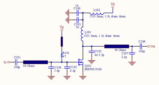
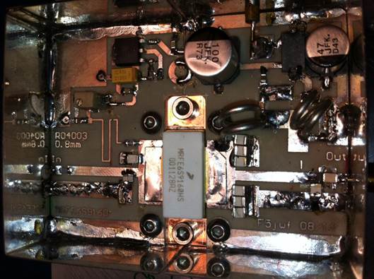
Figure 1: Principle schematic
My
optimized layout is shown in Figure 3, it fits into a Shubert box: 72mm x
54mm.
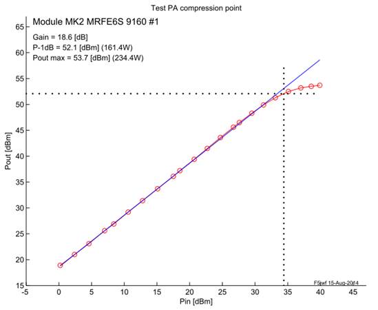
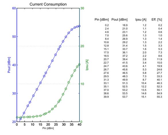
Measured performances are very interesting:
G~18.6dB, P-1dB~160W, S11
<-20dB, Vcc=28V 12A
|
|
|
|
|
Figure 2: Gain and power consumption of PA x1 |
|
|
|
|
|
|
|
Figure 3: PA x1 |
|
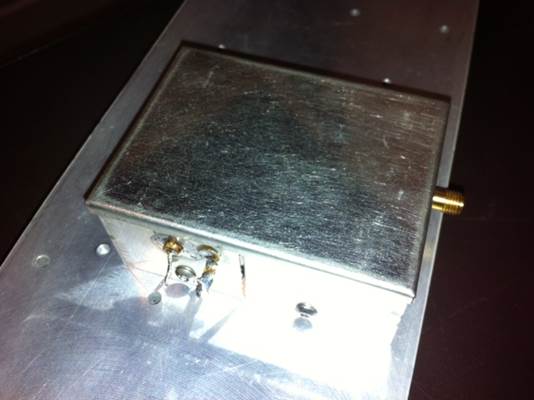
Figure 4: PA brick in box 72mm x 54mm |
From this
brick, few alternatives were possible, 2 or 4 transistors. Hennings
propose 2 transistors version, contact him for any information. On my side, I
have focused on a version with 4 transistors to reach 500W in a compact design
which can be integrated in my EME antenna. The
diagram of Figure 1 is repeated four times in
the 4-transistor design presented below.
On all of these versions of PA, the transistors are soldered on a solid
copper plate with a Eutectic melting at 138° (Edsyn
CR11, Sn42Bi58 see BOM for supplier). This operation is delicate but very
achievable with a hot plate set at this temperature. Be careful that such
device don’t live at all too hot temperature don’t heat them above 150…160°.
Be carefull with static, take care of grouding your working space, iron and yourself
The PCB is manufactured in two distinct parts then is screwed on each
side of the copper plate and then gate and drain soldered.
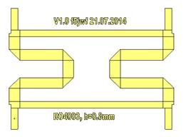
The substrate used originally by Henning is the RO4003, h = 0.813mm.
Similar results were obtained with Arlon 25N h = 0.76mm found at Franco Rota
(25N-30-22x114). http://www.rf-microwave.com/en/home.html
The MRF6S 9160 are currently available on Ebay at utsource for about 10 ... 15USD.
![]()
The hybrid
couplers required for the assembly of 4 transistors were optimized by simulation.
The simulation allows also to evaluate sensitivity of the trace width on the
balance of the channels. A few percent of tolerance (typ. 3%) over the width of
the branch 90° and 180° and they are quickly unbalanced of a few tenths of dB.
The length of lines acts on the resonant frequency.
The first
prototype is shown below. Coupling balance is very good.
|
|
|
S21=-3.3dB
@1.296MHz |
|
S31=-3.3dB
@1.296MHz |
||
|
S41=-28dB
@1.296MHz |
||
|
|
Figure 5: Hybrid Coupler x1
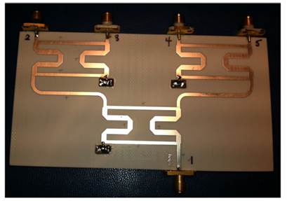
A x4
version has then etched to check the performance.
|
|
|
|
|
Figure 6: Coupler x4 |
|
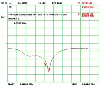
Figure 7: Resonance of x4 Coupler |
|
1.296MHz |
|
|
|
S21= -6.3dB, F= -89° |
|
S31= -6.2dB, F= -178° |
|
S41= -6.3dB, F= -89° |
|
S51= -6.3dB, F= 0° |
|
S23= -22dB |
|
|
The resonance
of the coupler is slightly shifted upward but remains fully usable in 1296 with
a return loss of -22dB.
![]()
Basically
the x4 design is a copy and paste of four times the Figure 1 including polarization (Figure 8) and hybrid couplers.
The PCB is
mechanically split into two to allow mechanical assembly. In the middle, the
copper plate is inserted with transistors that have been soldered. All other
components are mounted on the two PCBs in a first step, and then the two
circuits are screwed to the copper plate. At the end the gates and drains are
soldered to PCB. Quick tip, reduce the length of the legs of drain and gate to
about 3mm of the package and then solder. It makes no difference on performance
and it greatly facilitates any subsequent dismantling.
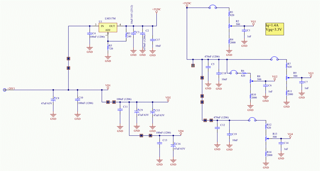
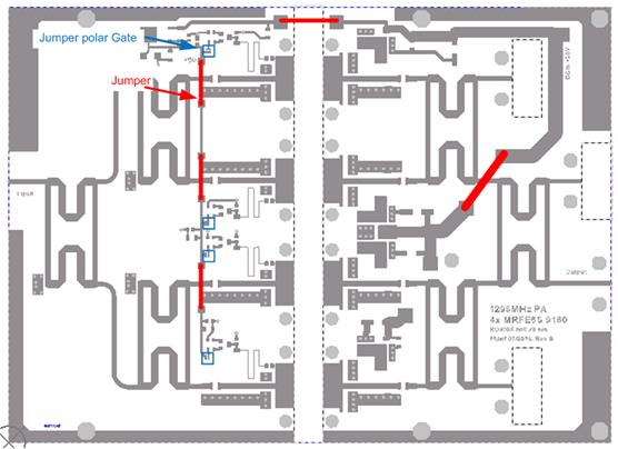
Figure 8: Polarization part
Mounting
phase, the following steps have to be done:
•
Installation
of polarization components of gates and drains following Figure 8 and Figure 9.
•
Mounting
matching and couplings ATC caps as shown in Figure 9.
•
The
inductors have to be made with silver plated copper wire diameter 1.5mm, wound
on 6mm drill bit to make 1.5 turns.
•
The
input SMD 50 Ohms loads are soldered directly on the PCB and the output one are
screwed on aluminum plate at the end.
•
A
few "jumpers " have to be mounted to
distribute the gate and drain voltage in the middle of the assembly (see Figure 11).
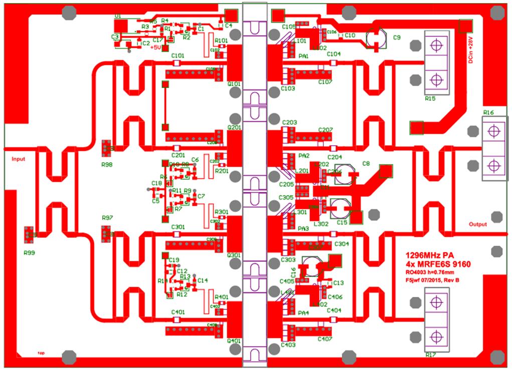
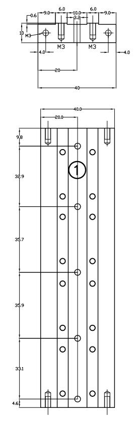
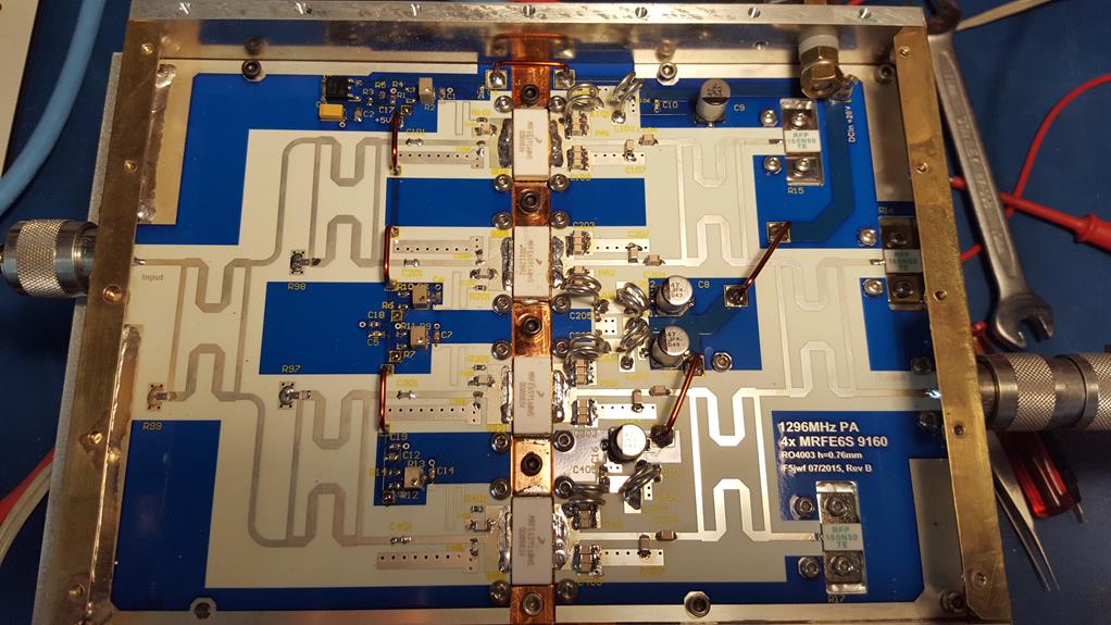
Figure 9: x4 Layout
The input
and output flanges are done with folded brass sheet to allow soldering the PCB
with N connector in order to improve RF transition (Figure 10).
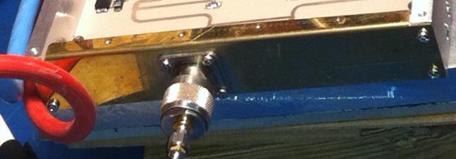
Figure 10: Input Flange
The PCB
backplane – Flange transition is soldered from below.
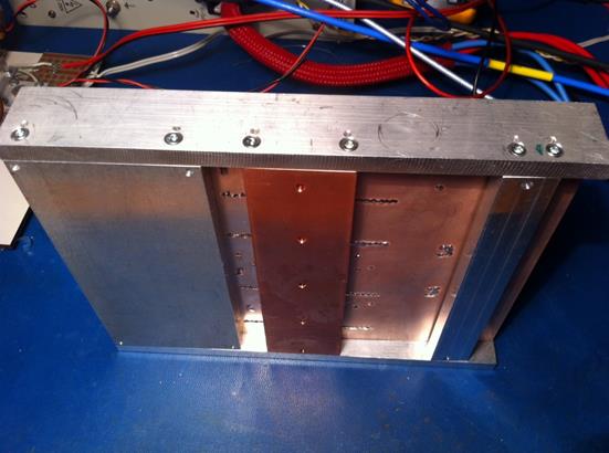
Are
distinguished on the bottom view of Figure 12, the copper plate of the transistors,
the aluminum plate which help to dissipate calories from outputs couplers, and
the reinforcement piece on input to mechanically secure the assembly. Two
lateral flats close the box.
|
|
|
|
|
Figure 11: “Jumper” position |
|
|
|
|
|
|
|
Figure 12: Mechanical bottom
view |
|
Figure 13: Copper Plate assembly |
Figure 14 and Figure 15 give details of the full assembly.
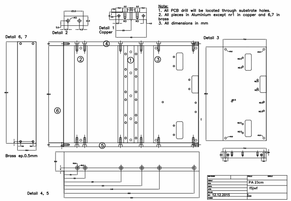
Figure 14: Mechanical
details

Figure 15: PA in operation on the test bench
![]()
The gate
voltage must be set to a drain current of 1.4A per transistor by using
potentiometers. This current corresponds to gate voltage of approximately 3.3V.
The current adjustment is a delicate point because the overall intensity of the
PA cannot be easily measured. For this purpose, welding jumpers have been
included which allow to interrupt the gate voltage and adjust the polarization
per stage basis (cf Figure 11).
Once the 4
transistors properly biased, low level RF can be injected (typically 100mW ) and measure the gain. In principle, there would be
nothing to adjust or retouch and it should peak to about 15 to 18 dB gain. It
could possibly be interested to check residual power on the load, using an RF
probe and verify that we have between 10 to 15 dB isolation.
When good
test results at low level are done then tests at sustained power can be
started, typically between 5 and 10W drive . This is
the tricky part and obviously there are several precautions to take:
•
Ensure
that the output load 50 Ohms hold that such power (max 600W)
•
Provide
cooling accordingly. Efficiency of these devices is only about 40% @1.2GHz. This
means that for 1400W (28V 50A) drawn off the power supply, 560W are the RF and
800 are heat that must be dissipated.
•
You
have to find solution to measure such power. I use a 40dB directional coupler
and a 1.2GHz 50Ohms load rated for 1kW.
•
Prepare
heavy duty (for serious guys) 28V power supply, the saturation power reaches
630W for a current of 65A.
•
At
the beginning, start with brief transmissions to detect potential problems
before the disaster.
•
Cautions
on your fingers, eyes and other attributes, the RF burns and such high levels
are not trivial. For my part, I never stay close to PA when running at full
power.
Optimization
is the major difficulty of this assembly because the four-way interact with
each other and mismatch occur into saturation region. It is therefore necessary
to optimize at maximum power. The position of the caps C107 (C207, C307, C407)
play on the output power and on the balance of 4 transistors. Playing with
position of these caps to optimize the linear region as large as possible. Figure 17 corresponds to the gain curve after
optimization. The 1dB compression point is more than 500W with a good linear
characteristic. This is the target after optimization.
Without
this optional step of optimizing, your PA will probably start compression at
400W (P-1dB) to reach its maximum power at 600W which is not very linear but
ultimately not a problem operation in EME CW.
|
|
|
|
|
Figure 17: Compression curve and
consumption of optimized prototype |
|
|
![]()
These MRF6S
9160 offer interesting solution for 23cm EME station, the design is compact,
transistors are cheap and with a little effort, 500 to 600W can be reached
allowing very good echoes with a 3…4m dish.
This design
is really to be reserved for OM already experienced with RF assemblies. Without
such skills you are exposed to profound disillusionment and pain.
The 28V
power supply is essential. Almost 70A will be required to exceed 600W. Such
large currents require special precautions rather unusual in electronics.
(Connectors, wire gauges, protections against short circuits, shutdown TX / RX
...). For my part I use the excellent design of 28V power supply by F5UAM which
I warmly recommend.
A small
series of PCB Silvered RO4003 was produced, if you are interested contact me.
This
prototype was mounted in my 23cm EME station with which I operated for the last
ARRL EME contest. 20 QSOs CW were made with RST ranging up to 579. The cooling
water circulation in the aluminum heat sink is very efficient and the temperature
never exceeds 30°C despite sustained transmission for several minutes.
![]()
Il will try to collect building experience
into a specific web page: PA_23cm_500W_tips_and_tricks
![]()
-
Station
EME 23cm F5jwf
http://f5jwf.free.fr/Station_EME_23cm.pdf
-
Neue
LDMOS-PA für 1296MHz Süddeutsches SHF-Treffen 05/2014
. (http://www.df9ic.de/doc/doc_chrono.htm)
-
utsource on ebay
http://www.ebay.fr/itm/10PCS-MRF6S9160HS-Encapsulation-RF-TRANSISTOR-RF-Power-Field-Effect-/131213143908?hash=item1e8ce9af64:g:AOUAAOSwyZ5Upil6
-
Alimentation QRO 26 à 30V / 50A F5UAM / F5JWF
Bulletin Hyper Numéro 128 Juillet-Aout 2007
http://www.revue-hyper.fr/bulletins/128.pdf