PA
23cm 500W 4x MRFE6S 9160
Assembly Tips & Tricks
Philippe Borghini / F5jwf
![]()
PA
23cm 500W 4x MRFE6S 9160
Philippe Borghini / F5jwf
![]()
Last
Update: 18.01.2019
![]()
Up to date docs to build the PA assembly, last update 18.01.2019: PA_23cm_500W.zip
![]()
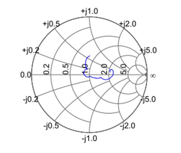
7.02.2016 S11, S22
measurements.
|
|
|
|
|
Figure 1: PA 23cm S11 |
|
Figure 1b: S11 Smith chart |
|
|
|
|
|
Figure 2: PA23cm S22 |
|
|
![]()
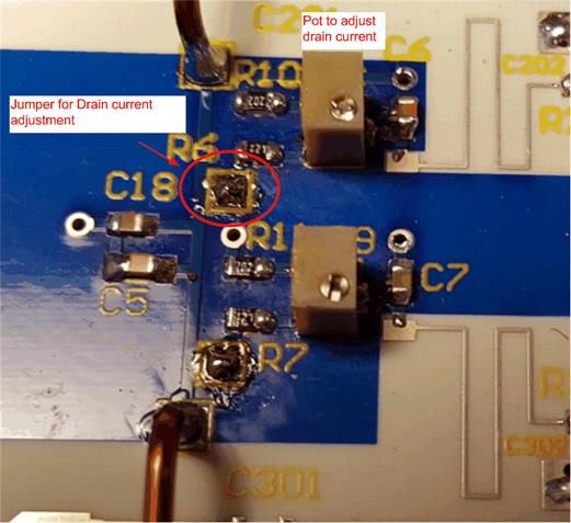
30.01.2016 Adjustement and test.
Before
applying +28V to the drain of the LDMOS pre adjust the gate voltage to around +3.3V.
Then +28V can be applied and current adjusted to 1.4A.
For this
purpose, measure the current on your power supply or on the wire feed with
current probe clamp and adjust current stage by stage. Jumper can be shorted
(Figure 1) or not to apply gate voltage and adjust only one LDMOS at time.
I have seen
pretty large dispersion in the gate voltage for 1.4A drain current: Vgate: 3.0…3.3V
|
|
|
Idrain=1.4A
Vgate~3.0 … 3.3V |
|
Figure 1 |
|
|
Once the 4
transistors properly biased, low level RF can be injected (typically 100mW ) and measure the gain. In principle, there would be
nothing to adjust or retouch and it should peak to about 15 to 18 dB gain. It could
possibly be interested to check residual power on the load, using an RF probe
and verify that we have between 10 to 15 dB isolation.
When good
test results at low level are done then tests at sustained power can be
started, typically between 5 and 10W drive. This is the tricky part and
obviously there are several precautions to take:
•
Ensure
that the output load 50 Ohms hold that such power (max 600W)
•
Provide
cooling accordingly. Efficiency of these devices is only about 40% @1.2GHz.
This means that for 1400W (28V 50A) drawn off the power supply, 560W are the RF
and 800 are heat that must be dissipated.
•
You
have to find solution to measure such power. I use a 40dB directional coupler
and a 1.2GHz 50Ohms load rated for 1kW.
•
Prepare
heavy duty (for serious guys) 28V power supply, the saturation power reaches
630W for a current of 65A.
•
At
the beginning, start with brief transmissions to detect potential problems
before the disaster.
•
Cautions
on your fingers, eyes and other attributes, the RF burns and such high levels
are not trivial. For my part, I never stay close to PA when running at full
power.
Optimization
is the major difficulty of this assembly because the four-way interact with
each other and mismatch occur into saturation region. It is therefore necessary
to optimize at maximum power. The position of the caps C107 (C207, C307, C407)
play on the output power and on the balance of 4 transistors. Playing with
position of these caps to optimize the linear region as large as possible. Figure 17 corresponds to the gain curve after
optimization. The 1dB compression point is more than 500W with a good linear
characteristic. This is the target after optimization.
|
|
|
|
|
Figure 2 |
|
|
|
|
|
|
|
Figure 3: Automatic Test setup measurement Pout vs Pin |
|
|
![]()
15.01.2016 Build of the first
PA with released PCB.
The copper plate
has to be drill according to mechanical drawing.
|
|
|
|
|
Figure 1: Drilling the copper plate |
|
|
For accuracy,
the PCB is used to locate the holes in backplane plates.
|
|
|
|
|
Figure 2: Mechanical parts |
|
Figure 2b: Input flange in brass bended |
It is a
good practice before soldering the device to check them with DVM
|
|
|
When device failed I usually seen:
|
|
Figure 3:Internal model of LDMOS and LDMOS Ohmic Test |
|
|
The LDMOS soldering
is the FUN time…Here are the step to follow:
|
|
|
|
|
Figure 4: Good quantity of solder paste is important |
|
Figure 5: Device soldered |
|
|
|
|
|
Figure 6: Solder paste preparation |
|
Figure 7: Hold the devices during the soldering process |
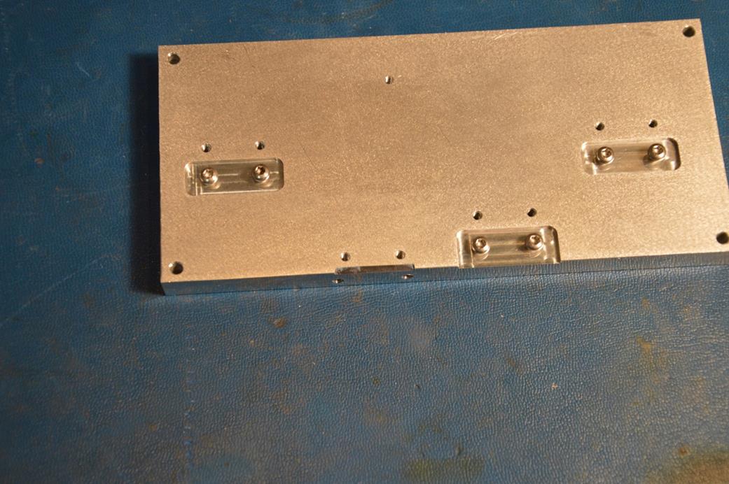
The output aluminum
plate has to be prepared to hold the 50ohms load.
|
|
|
|
|
Figure 8: Output Aliminium plate |
|
|
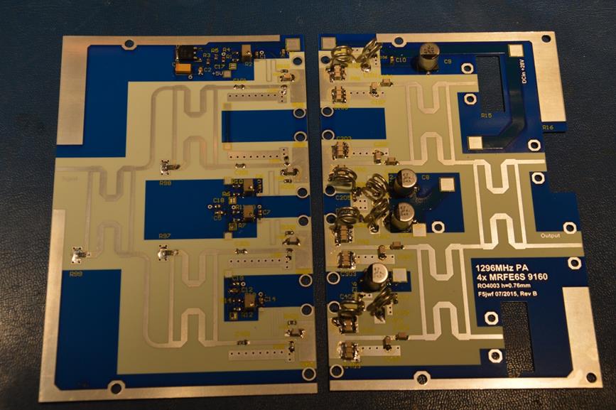
All components
can mounted on PCB before final mechanical assembly.
|
|
|
|
|
Figure 9: Two part PCB equipped with component |
|
Figure 9b: Details of the coils |
Input
connector, brass edge and PCB backplane can be soldered together (Figure 9) for a perfect RF transition.
It is
difficult to do the same on output connector because the aluminium
plate. Solution could be to use a small piece of copper sheet (0.1mm thick)
bend it around PCB edge (Figure 11) solder it on the backplane with
minimum paste to avoid thickness. Then you are able to solder it to the brass
edge from top of PCB
for a perfect RF transition. Other solution are also possible as 1.2GHz are not
so critical.
|
|
|
|
|
Figure 10: Input connector details |
|
Figure 11: Input connector details |
For the
output connector, it is difficult to do the same as input because the aluminium plate are close to edge of brass flange. Solution
could be to use a small piece of copper sheet (0.1mm thick) bend it around PCB
edge (Figure 12) solder it on the backplane with
minimum paste to avoid thickness. Then you are able to solder it to the brass
edge from top of PCB
(Figure 13) for a perfect RF transition. Other
solutions are also possible as 1.2GHz are not so critical.
|
|
|
|
|
Figure 12: Output connector backplane detail |
|
Figure 13: Output connector |
Before final
assembly check every fit well together, then add thermal compound paste on the
output aluminum plate (Figure 12)
|
|
|
|
|
Figure 14: Thermal compound paste on output aluminium plate |
|
Figure 15: Thermal compound paste on 50Ohms load location |
At the end
remaining item can be mounted:
·
Brasse edge
·
Jumper
·
+28V
bypass
·
Output
50ohms load
·
Solder
the gate and drain of the LDMOS
|
|
|
|
|
Figure 16: Final assembly ready for test |
|
|