


The first stage is based on FLC253MH driver followed by two FLM7177-4 power FET.


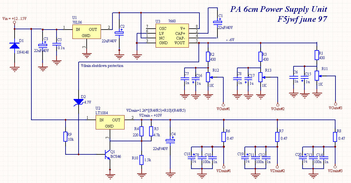
The power supply is based on 7660 negative DC converter which produce Gate voltgage for the 3 power FETs. The Drain is powered trought LT1084 serial regulator. A security signal avoid Drain voltage in case of Gate voltage failure.
RF Adjustement:
1° Adjust 2nd stage without first stage mounted. Inject small power and add stub to get max power on output and min power on reflected output. 7..8dB gain should be measured with standard device.
2° Mount driver FET and add stub to maximise outup power.
3° Increase input power to found 1dB compression point.
4° Optimise stub position at full power


P-1dB = 8.7W (39.4dBm) at gain=14.6dB
Rlin~-20dB Bandwidth~240MHz (4%)
Power consumption = 2.3A on 13.8V
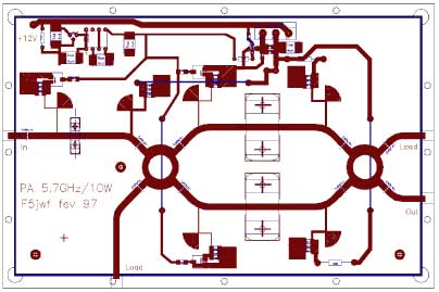
The PCB file on electronic format could be ask on my e-mail adress.

