Wide band power detector to control microwave
station
by Philippe Borghini /
F5jwf
April 19th 2010
Introduction
Everyone knows the famous logarithmic detectors from
Analog Device. So many designs have been done with the well
known AD8307. These
kinds of circuits provide a dc voltage proportional to the RF signal expressed
in dB. Analog
Device expands recently his detector family with the ADL5519 which is still
usable at 10GHz.
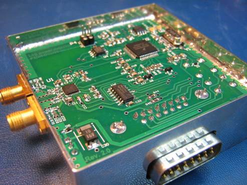
The assembly presented below integrates a dual channel
power probe by using the ADL5519. This design provides a control unit to
measure the output power of microwave radio station. His enhanced linearity
makes it also valuable as a good alternative to the old HP432 RF power probe to
any Ham microwave labs.
Block Diagram
The particular interest of the ADL5519 is focused on
bandwidth which is specified up to 8GHz (but still usable in 10GHz with reduced
dynamic). With two channels, it is possible to measure the power transmitted to
the antenna and the reflected wave, to calculate the return loss and block the
PTT when problems arise. As I originally destined it to my EME 13cm station the
module is controlled remotely by serial interface (RS232 and RS485) to be
installed in the antenna 30m away the shack. A simple RS232 VT100 terminal
allows the full control of the assembly as the whole software is embedded.
The set also includes some additional features such as
measuring the temperature of the PA with KTY probes and power supply voltages.
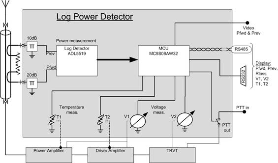 Figure 1: Block diagram of DetLog
module. Logarithmic detector and Micro Controller Unit (MCU).
Figure 1: Block diagram of DetLog
module. Logarithmic detector and Micro Controller Unit (MCU).
The RF coupler remains external to the detector and
can be done either with semi rigid coaxial cable or with commercial device. The
coupling factor is taken into account by the software and can also be included
in the calibration process.
Typical
Applications of the DetLog board
Control of 13cm F5jwf EME station
Linearity and dynamic
Without calibration, the linearity of the ADL5519 is
already excellent. The frequency behavior is also fairly flat but a calibration
specific to each frequency can improved a little bit the linearity. The dynamic
is around 50dB for an accuracy of +/- 0.5dB. Isolation between two channels is
better than 40dB.
Figure 2 shows the ultimate accuracy obtained at 1296MHz +
/ - 0.1dB over nearly 40dB.
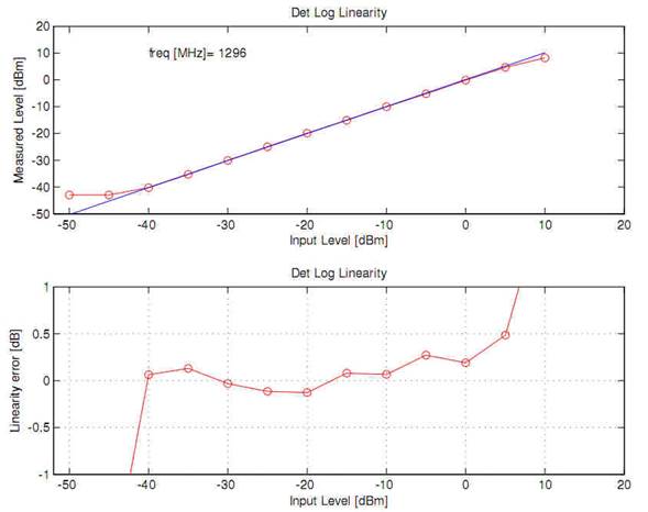
Figure 2: Linearity at 1296MHz.
The curves for other frequencies are quite similar:
Up to 8GHz, the dynamic of 50dB is guaranteed. Above
this frequency the sensitivity decreases and more power is needed for the same
detected voltage. The linearity is also a little bit degraded but the detector
is still usable as PA controller.
The input impedance of the detector chip is equivalent
to 2kOhms load in parallel with 0.6pF. Loaded with a resistance of 50 ohms on
the input, we obtain acceptable impedance up to 2 GHz but degrade rapidly
beyond. The input attenuation pad can significantly improve the return loss and
the broadband performance. The layout has two
10dB pad achieved with 0402 SMD resistors. These pads can shift up the dynamic
to 10 or 20dB increasing the compression point respectively to 10dBm or 20dBm. Obviously
this comes at the expense of sensitivity.
It is advisable to have at
least 10dB to ensure a good matching of the input. The maximum power rating of
10dB attenuator made with 0402 SMD resistor is around 100mW, beyond an external
attenuator must be added.
An optimum configuration in terms of dynamic and sensitivity for return loss measurement is 20dB attenuation on the forward channel and 10dB on reverse channel. This option gives the following dynamics:
Channel
Forward: Dynamic~ -30dBm…+20dBm S11~ < -23dB for f=144M...10GHz
Channel
Reverse: Dynamic~ -40dBm…+10dBm S11~ < -20dB for f=144M...10GHz
Note: 10dB attenuation seems to be an optimum of flatness for an attenuator
in PI with regular SMD package. This value corresponds to resistances value
between 70 and 100 ohms. Outside these limits the behavior of capacitive or
inductive SMD package dominates and introduces resonances.
Calibration
The calibration process is the action of
putting a well known level at the RF input and entry
this level to the microcontroller to correct the measurement error. Of course
few points are necessary to obtain good correction and those are frequency dependant. The calibration algorithm finds then the best
linear regression minimizing the error over the full dynamic. This process is done by an external test bench based
on RF synthesizer and commercial power meter, taking about 50 points Vdetected = f (Pin), and calculating the gain and offset
for each frequency. These values are then stored in
Basically for the kit proposed below two calibration are possible:
. Default standard cal (kit#1 and kit#2) accuracy around typ. +/-0.5dB up to 1.2G and typ +/- 1dB for higher freq.
. Calibration dedicated to the DetLog board mounted and tested only possible on kit#3. Then the accuracy is around +/- 0.2dB
Remark:
The calibration algorithm does not work
on the frequency axis. It means that between two calibrated frequencies no
correction is done.
Example: If you want to measure at 3400
MHz you have to use the closer cal, let say 2320 MHz
and then correction is not optimal.
You could run the built in calibration
process at 3400 MHz to calculate the linearization parameters at this frequency
and save it on one free memory.
The built in cal
use up to 8 measurements points to calculate the linearization. This procedure
can also be used to take into account external
attenuator or coupling factor. At the end of the process the cal parameters are saved into the current cal memory which is located in ROM (no volatile after power
off). A total of 9 memory banks are
available to save calibration for further uses.
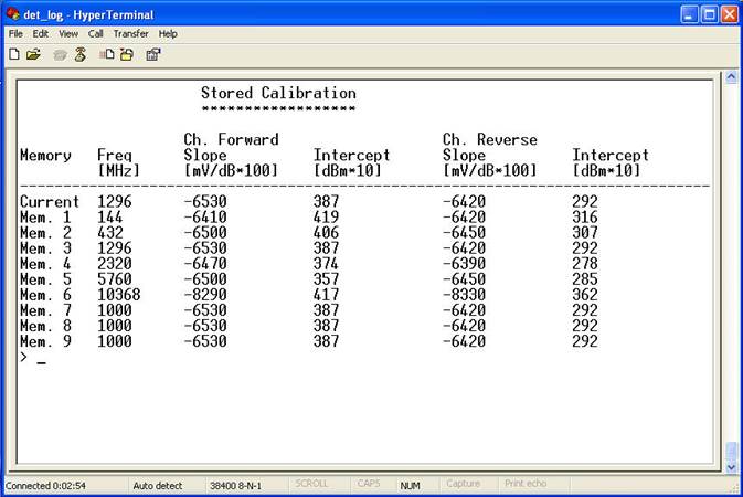
Figure 3: The calibration factors for one specific frequency can be reloaded with the VT100 terminal
A simple offset to the
displayed value is also configurable to take into account such as a directional
coupler factor or an external attenuator.
Voltage and temperature measurements
The DetLog PCB measures also voltages and temperatures
of power amplifier. Two channels are available:
.
Voltage 1: Resistif divider 1:7.8 Input= 0…40Vdc
.
Voltage 2: Resistif divider 1:7.8 Input= 0…40Vdc
.
Temp 1: KTY-10-6
temperature sensor Temp=-20…100°C
.
Temp2: KTY-10-6
temperature sensor Temp=-20…100°C
A PWM (Pulse Width Modulation) output can be connected to
control the speed of the FAN. The speed is controlled by the software according
to the temperature Temp1.
VT100 User Interface
Measurements of power, temperature and voltage are
displayed directly on the terminal screen (VT100 emulation commonly available
under any OS). The different functions are handled by the terminal and are
summarized in the on-line Help. The Return Loss limit for example is configured
with the terminal. Above this configured level the module open a relay to block
the PTT.
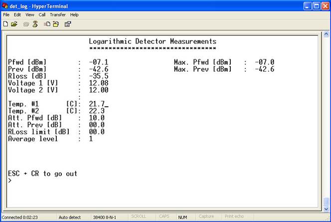
Figure 4: Main page on the RS232 terminal. Current and "max. hold" power is displayed in dBm. PA voltages and temperatures. The display is refreshed
every 100ms.
Video outputs
Two analog outputs (one for each channel) giving an
exact replica of the measured power is available as a DC signal varying from 0 ...
5V for the total detector dynamic. They can drive analog meter or external XY
plotter.
The RS232 port can also be used for automatic measurement
bench and power points can be transferred in third-party software.
VT100 Commands descriptions
The built in help is access on the RS232 port by typing
?. The Figure 5 and Figure 6 are then displayed.
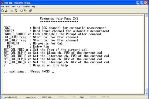
Figure 5: Online help is displayed on the VT100 terminal with the ? command.
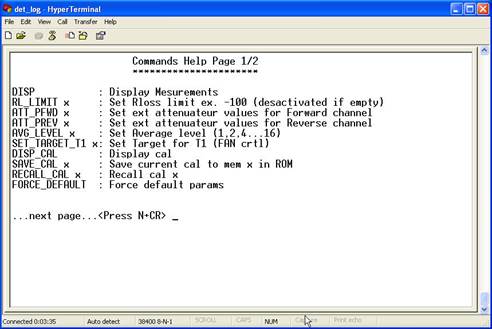 Figure 6: Page 2 of the help.
List of
the command
Note 1: All command are NOT case sensitive, they can be either upper or lower case independently.
Note 2: The format to entry attenuation in dB (or power level in dBm) is on 3 digits without decimal point.
Example: To entry the attenuation value of -12.5dBm you have to entry -125
|
Command |
Explanation |
Example |
|
DISP |
Display the main panel with the measurement. Escape and carriage return allows to go out of this page. |
|
|
RL_LIMIT x |
Set the Return loss limit. If the measured Return loss exceed this value the micro relay open which block the PTT of the station. |
x = -85 for RL max of -8.5dB. If measured RL is -5dB, the PTT will be blocked to protect the PA. |
|
ATT_PFWD x |
Set the value of the external attenuator for forward channel. Negative value represents attenuation. |
x = -100 for external attenuator of -10.0dB |
|
ATT_PREV x |
Set the value of the external attenuator for reverse channel. Negative value represents attenuation. |
x = -100 for external attenuator of -10.0dB |
|
AVG_LEVEL x |
Set the value averaging. When measurements are close to the noise, average can be increase to higher value to improve measurement confidence. |
x =1, 2, 4, 8, 16 |
|
SET_TARGET_T1 x |
Set the temperature limit for temp1. When the temperature measured by the probe temp1 will come close to this limit, the controller will increased the speed of the PA fan by increasing the duty cycle of the PWM. |
x =430 for a temperature limit of 43°C |
|
DISP_CAL |
Display the calibration table. |
Cf. Figure 3 |
|
SAVE_CAL x |
Save the current calibration into memory bank x. |
x=1…9 |
|
RECALL_CAL x |
Recall the calibration of memory bank x into current cal. |
x=1…9 |
|
FORCE_DEFAULT |
Set all variable of the controller to factory settings. Could be useful when bad parameters have been entry. Following this command, the factory standard cal is reloaded and custom cal lost. |
|
|
ADC? |
Request to get the ADC value (10bits) of the RF detector. The result is express in microvolt. |
Vdet_Pfwd=4562000 Vdet_Prev=2350000 |
|
POWER? |
Request to get the measured power of both channels. The result is express in dBm *10. The command can be used in automatic test setup to read the power level. |
Pfwd=-245 Prev=-372 |
|
PROMPT_ENABLE x |
In normal situation, the controller answer to each command with a prompt symbol which is >. During automatic measurement when the module is pooled by tiers party software, disabling the prompt avoid complicated ASCII stream handling. With x=0 the prompt is not send anymore. |
X=0 or 1 |
|
CAL_PFWD freq |
Start the build in user calibration process. The software expect that you connect RF source and you entry the power level. |
CAL_PFWD 1296 |
|
NB_POINT x |
This command works with the previous "CAL_PFWD freq" command and allows to entry how many points is used for the calibration. The maximum points for the built in cal in 8. |
NB_POINT 4 |
|
PIN x |
This command works with the previous "CAL_PFWD freq" command and allows to entry the value of the power level you just connect to the input port. The maximum dynamic is -70dBm…+20dBm. Remember that the format for level must comply with Note 2 |
PIN -200 (for -20.0dBm) |
|
CAL_PREV freq |
Same command as CAL_PFWD freq for the channel reverse. |
CAL_PREV 1296 |
|
SET_CAL_FREQ x |
Allows to entry the frequency for the current cal. |
SET_CAL_FREQ 1296 |
|
SET_CAL_SLP_F x |
Allows to entry the cal SLOPE cal parameter for the current cal. It is expressed in dB/mV *100 as shown in Figure 3. |
SET_CAL_SLP_F -6472 |
|
SET_CAL_INT_F x |
Allows to entry the cal INTERCEPT cal parameter for the current cal. It is expressed in dBm *10 as shown in Figure 3 |
SET_CAL_INT_F -395 |
|
SET_CAL_SLP_R x |
Same as SET_CAL_SLP_F x for reverse channel. |
SET_CAL_SLP_R -6472 |
|
SET_CAL_INT_R x |
Same as SET_CAL_INT_F x for reverse channel. |
SET_CAL_INT_R -395 |
RS485 Bus
 Since few developments, F1TJJ and I start to
implement RS485 communication between our HAM radio modules. As this two wires
protocol is differential it allows transmitting easily few ten of kbps over
very long twisted pairs. Stephane also implement the MODBUS (protocol level 2)
which run over the rs485. This solution provide a frame oriented communication
with error detection and device addressing over the bus.
Since few developments, F1TJJ and I start to
implement RS485 communication between our HAM radio modules. As this two wires
protocol is differential it allows transmitting easily few ten of kbps over
very long twisted pairs. Stephane also implement the MODBUS (protocol level 2)
which run over the rs485. This solution provide a frame oriented communication
with error detection and device addressing over the bus.
To keep simple,
the DetLog module just attached itself on this two
wire and can be remotely controlled by using a small piece of software running
on windows XP.
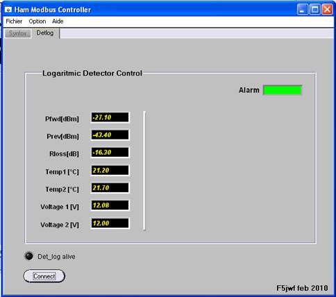
Figure
7: Windows XP HAM
Modbus Controller application
Design and Layout
The schematic of the module is shown on the Figure 7 to Figure 9. It is a very standard application of the detector and of the MCU devices and nothing special has to be said. Only a few additional circuits allow interfacing with outside world. The module is powered with a single 12V dc power source.
Remark: These figures here below give an overview to present the module. To be sure to have the up to date version use the pdf design folder
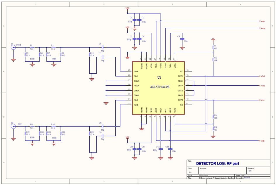
Figure 8: Schematic part 1: Detector with 10dB attenuator pad.
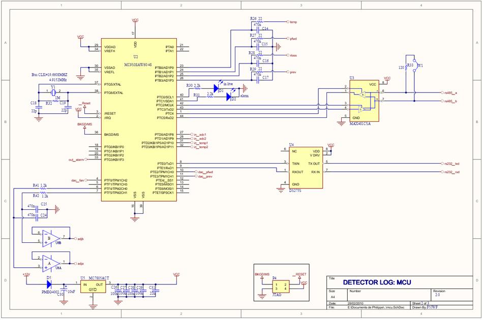
Figure 9: Schematic part 2: MCU with serial interfaces RS232 and RS485
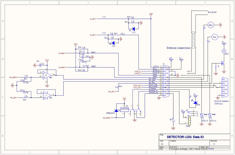
Figure 10: Schematic part 3: Interface components. Standard DB15 connector is used for control signals. On the right of the DB15 the external component (KTY temp. probe, PTT relay,…) can be seen.
The layout is done on printed circuit board
FR4 double sided plated holes of 0.8mm with serigraphy on both side. The PCB
can be soldered in a standard 74x74 Schubert box. Most
components are SMD 0805, 0603 and 0402 for input attenuators.
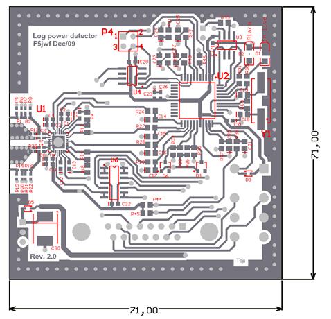
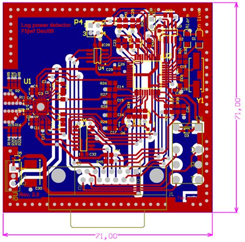
Figure 11: Two side PCB Layout. TOP layer in red and Bottom in blue. Figure 12: Component view. Almost all parts are soldered in the TOP layer.
Bill of
Material
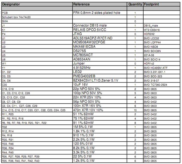
Document up to
date ready for download
Download the Up to date Design Folder in pdf
Configuration file for Windows Hyperterminal
Mounting guidelines
All parts are SMD, they have to be soldered carefully but this kit is definitely within the reach of any HAM radio who is experienced with assembly in the RF and microwave band. The most sensitive step is the soldering of the detector ADL5519. The best practice from my experience is to use SMD solder paste and heat up with hot gun. The chip is then auto centered into the pad and is magically done. The details of the mounting are explained in the design folder above. The following video give an idea how to deal with this step.
Soldering of the ADL5519 (35MB)
Conclusions
In terms of dynamics and accuracy, this detector is a
good alternative at affordable price of most sensors available at flea markets.
The DetLog board provides
functionalities which can be used in a lot of application like power amplifier
control, labs power measurement, antenna gain measurement with competitive
accuracy. It can be easily interfaced trough serial interface for automatic
test bench.
A big part of my time in this development has been used
for software design, I really want to thanks Stéphane
F1TJJ (http://www.ham-hyper.com/) for his great
support during this phase.
Kit availability
I have organized myself to propose the following kits:
|
Kit#1: PCB and
special parts |
|
Price 40 euros |
|
PCB , microcontroller MC9S08AW32 programmed with standard
calibration, Detector ADL5519 |
||
|
Kit#2: Kit with all
parts |
|
Price 90 euros |
|
PCB, microcontroller MC9S08AW32 programmed with
standard calibration, Detector ADL5519, all parts according to the BOM,
including drilled Schubert box but except the two input SMA connectors. |
||
|
Kit#3: Fully
assembled and tested |
|
Price 250 euros |
|
Detector box fully assembled, tested calibrated
(accurate cal). Each module is calibrated and
delivered with calibration sheet. |
||
Those kits can be ordered to my email address:
![]()